
Colourful coatings on Aluminium surfaces at Okuno booth – 2018 nanotechnology exhibition

Tokyo Big Sight Exhibition Center

Group Photo of Team Nano with staff from the NEC booth – 2018 nanotechnology exhibition

Nanotechnology Study Tour – 2018
La Trobe and NUS students visiting Tokyo, Japan in February 2018


My outlook for my future career has improved. This has been a very positive experience and will look really good on my resume. It has become clear to me the important of understanding the principle and workings of scientific equipment is. In future I will try to gain as much exposure to as many instruments as possible. I also think that nano-coatings may become a really big thing in future years and a promising area for me to work in.
I enjoyed the study tour. I think the amount of work required is appropriate, however having to write a journal and a blog every night was draining. The long days where physically draining and the workload was emotionally draining. By the end of the week I was well and truly ready to go home. I would have enjoyed myself more if I only had to write the blog post, and was able to go out in the evening to explore rather than be stressed out about the amount of work required of me every evening.
Meeting the students from Singapore was interesting, they certainly have a different way of doing things. This was a good way to approach a project with a different mindset and open myself up to their way of completing the project. Being put in a situation where I have to communicate with a person who speaks another language was challenging, but I think it has improved my communication skills. Working with a group has also improved my communication and team working skills. So far my team has cooperated very well and we have all contributed equally toward the project.
I always try and take a life lesson away from my travels after opening my eyes to how people in other countries go about their lives. I think from Japan what I will take away is politeness, it costs nothing to be kind, respectful and polite and it will always give something positive to another person. In future I will endeavour to be more kind and understanding.
Its always nice to come home when these two are here to greet me.

Today we spent the entire day at the nanotechnology exhibition. There were over 700 exhibits to see. I spent most of the day walking around collecting pamphlets and talking to people. Most companies there were selling scientific instruments like atomic force microscopes, but there were also several stalls selling nano-coatings for materials like aluminium, catalysts and nano-structured carbon like graphene or nano-tubes all of which were unique and innovative.
In the morning I wrote the interview which we conducted with a researcher from NEC for our group project. I then continued to explore some of the other areas of the exhibition like the 3D printing and the smart energy exhibits.


The 3D printing exhibits were interesting. I didn’t realise how slow the process was. I also didn’t realise how much the quality varies based on the print time and material. It is worth noting that all the companies that I recall were either selling instruments or chemical catalysts or coatings. Which means that if I want to work for a company in the future these are the best directions to head during my studies. I must say, some of the coatings were really beautiful. That is the direction which interests me most.

Coloured coating for alimunum
I think I would have enjoyed the exhibition more if it was in English or if I could read Japanese. There were many posters and due to the language gap it is difficult to converse with people about their products. Given the nature of the exhibition, I felt like I was wasting peoples time. I was not there to buy anything or help the companies, I was there for my own benefit. It made it difficult for me to feel confident when approaching a stall. After the exhausting week walking over 20,000 steps a day, I was also in a lot of pain and my new fancy dress shoes were not helping.

Today we visited the Komaba campus of Tokyo university. We toured the Atomic force microscopy (AFM) lab where RGB colour AFM was being developed, we also saw the scanning electron microscope that was coupled with an AFM and hand held AFM, locally know as palm-AFM.


We then toured another lab which used Kelvin Probe microscopy (KFM) to conduct photovoltaic analysis of solar cell materials. They had also developed a way to collect rough AFM scans at 10 times the speed of a regular AFM scan.
After lunch we travelled across to Tokyo Big Sight to the nanotechnology exhibition. We interviewed our chosen small company Alkali, however the man present only spoke Chinese, so it was lucky that a few of the other students in my group were able to conduct an interview with him. I video taped the entire 40 minute interview without understanding a word of what was going on.
I then attended three seminars as a part of the special symposium on graphene. The first talk was given by Haydale who seem to have integrated graphene into many products, improving their functionality. The second seminar was given by Carbon Waters who have successfully dissolved graphene in a water solution by de-gassing the water and creating a stable colloid. They also print thin films on surfaces. The third seminar was given by Ctechnano. They use atomic layer deposition to create a thin film on a 3D surface. They are able to create a homogeneous layer without a shadowing effect using this technique; furthermore, by heating a polymer, they are able to expand the material slightly and create pores which can also be coated, altering the physical properties of the material.
By being put in a situation where I have to communicate well with a group and sell myself to exhibitors, I feel that I am becoming a better communicator and more confident in my ability to hold a conversation.
It is the start of a brand-new day where we troughed through the weather of Japan mornings. It seemed like second nature to dress warmly. However, today despite the low temperature, it did not feel as cold as it was compared to the previous days.
The schedule for today was a continuation of exploring the University of Tokyo. This time at Konaba Campus. Komaba campus homes the College of Arts and Science, the Graduate School of Arts and Sciences, the Graduate School of Mathematical Sciences and advanced research facilities. The Komaba campus is unique as it houses more than 7000 students in their freshman and sophomore year. The students will then choose their majors after the second year. The Institute of industrial science was the place of visit. We were introduced to the Nano-probing Technology in Prof. Takahashi Lab where we learn about the various microscopy techniques used to characterise the nanomaterial synthesised.
The most common spectroscopy is using Scanning Tunnelling Microscopy (STM), Atomic Force Microscopy (AFM), Kelvin-Force Microscopy (KFM) and Magnetic Force Microscopy (MFM). STM uses a current to detect the surface morphology whereas the other force microscopy uses the detection of force. We were given an introduction to the working principles of an AFM and some of its current research interest. Different research would use a different type of analysis and characterisation method.
In the multiple analysis of solar cell materials, the photovoltaic analysis is conducted using a KFM and a local photo-thermal spectroscopy by AFM. The KFM measure the electric potential by applying an electric bias between the sample. This allows for surface potential analysis which can be applied to solar cells as mentioned above. For solar cells, when exposed to light illumination, it is possible to localise the characterisation of the solar photovoltage distribution around grain boundaries. For a multi-crystalline silicon, the photovoltage measured will degrade underexposure and it can be seen as the appearance of recombination centres. However, in Cu(InGa)Se2 it is inactive when exposed to illumination. The grain boundaries no not degrade. This is, therefore, a measure of the stability of solar cells and its ability to undergo many cycles before degradation occurs. I was awed at the application of a simple microscopy technique to be able to analyse the characteristic for different properties of the materials. A photothermal spectroscopy AFM measures the expansion of material due to light. I have never heard of such a measurement before and was intrigued by the ability for them to change photon energy to allow for selective radiation. Restriction of the band gap is required for not radioactive recombination detection. This awesome spectroscopy, microscopy method made me think if Singapore has these facilities to support the machines.
![IMG_1642[1].JPG](https://nanotech2018.files.wordpress.com/2018/02/img_16421.jpg?w=525)
Image of the one of lab visited at the University of Tokyo, Komaba.
Another research project that made me feel that Japan has the best research facilities is their development of new SPM functions. In our lab in NUS, the AFM takes roughly about 2 – 5 minutes to scan for a small area small of about 0.3 nm by 0.3 nm. Whereas in Japan, the fast scanning AFM allows for a scan rate of 10 Hz/line. This would translate to around 30 seconds per sample. This is insanely faster! The modification to the AFM circuit was done. An additional add-on of an S/H alternate circuit. This addition of a circuit does not require a feedback loop which greatly slows down the process. This allows for fast imaging to potential landscape of surfaces and regulation of cantilever deflection was used to decrease thermal draft. This allows imaging to be more precise and less elongation due to thermal drift. It was really amazing to learn about the ways these researchers wanted to increase scanning rate and the results that came along.
![IMG_1688[1].JPG](https://nanotech2018.files.wordpress.com/2018/02/img_16881.jpg?w=525)
Using S/H sampling circuit to obtain AFM image.
After the introduction of working principles, we were brought into the labs to witness with our own eyes the spectroscopy machines and how did they build the entire set up. During the lab visit, we were introduced to a liquid AFM where a mirror is placed 45o with the cantilever in a vertical position. Currently, they are also trying to make the cantilever of about 8 Å for better detection and accuracy.
The visit to Komaba campus in the University of Tokyo was rather more on the educational side where we learn the techniques and application of different microscopy techniques.
After which, we proceed to make our way to the Nanotechnology Exhibition. I was excited to be here again as yesterday’s visit was too short and insufficient for me to enjoy and appreciate the entire exhibition. I visited entire exhibition and was very surprised at the difference between the researches done in schools and at industrial level. For me the most distinctive difference was the attitude towards different material, compounds, etc. For researches, we aim to find novel materials t improve our current problem yet these ideas are not able to take form immediately many companies are still very reliant conventual materials. Even some material where researches have deemed as not effective, not efficient, not reliable. Companies are still exploring to mass produce the old materials. The difference between research and demand in the world is different. Companies strive for lowest production cost possible whereas researcher aim for efficiency reliability of a materials. It is hard to find a company that would want to achieve both aims.
![IMG_1669[1].JPG](https://nanotech2018.files.wordpress.com/2018/02/img_16691.jpg?w=6528)
Overall the trip was inspiring as the seminars given out during the exhibition showcase the many possibilities and potential of the nano industries. It seems to have made my future slightly more bright with varying possibilities. I have also learnt that it is required for us to be flexible and think critically about the industry. Current industry may seem to be declining however, you have to look at its potential to determine whether the industry is truly declining or due to other reasons such as less funding, etc. Therefore, it was truly an eye-opening experience where I could spot and appreciate the difference and the gap between companies and researchers. Think twice if you think your invention can change the world! Will you even live to see that happen?

Today we travelled to the Hongo campus of Tokyo university. We toured two of their science labs the laser lab where they are using terahertz laser to measure the properties of superconductive materials and their phase changes by altering their excitation states, and the solid state chemistry labs which had created a transparent conductive material using laser deposition. We also visited the cryogenic research centre which recycles the liquid helium used across 60 laboratories by capturing the used helium in their ventilation systems, purifying the gas and the cooling the gas into a liquid and transferring it into smaller containers for transportation. This system has a 90% retention rate and can cool 20 litres of helium an hour. The University of Tokyo had some interesting health and safety practices; for example when entering a lab we were required to remove our shoes and out on ‘lab slippers’. While this is unusual in Australia, apparently it is to reduce the amount of dust inside the lab. I also saw a man transferring samples using the stairwell. Tokyo university also offers a masters + phD program which sounds amazing, but given that I am already enrolled in a masters degree in Australia and I am not sure I want to get a doctorate, I am not sure that it is for me.

Laboratory at the Hongo campus of Tokyo University
We then travelled across Tokyo to get to the Tokyo Big Sight exhibition centre. The building is enormous, much bigger than it appears from the outside. Once we registered we entered the exhibition hall. I must admit I was a bit overwhelmed by the amount of exhibits and people inside the hall. The map was on an A2 sheet of paper. There were many exhibitions giving out freebies in exchange for business cards. We spent the afternoon interacting with the exhibitors and collecting pamphlets, and then caught the ferry back to the hotel. The Tokyo university campus was very beautiful and resembled Melbourne University. It did not feel like Tokyo. All the buildings were spread out and it was very quiet.
The exhibition was a bit difficult to navigate, it was so large and once the exhibitors found out we were students and not interested in buying product, they became less interested in speaking with us.

Tokyo Big Sight Exhibition Center

Today we started early and took the express train to Tsukuba. After arriving at Tsukuba we were met by Dr. Andreas Doenni, who took us on a bus to the International Centre for Materials Nanoarchotectonics (MANA) at the Namiki Site of the National Institute of Materials Sciences (NIMS). We spent the morning listening to presentations about the overview of NIMS; its facilities and academic achievements, the student programs available through NIMS and MANA, how it is structured, its funding and its goals. MANA really pushes for inter-disciplinary collaboration, which is a really great way to forge new ideas and research by having someone challenge your views and your current way of thinking. It also encourages international collaboration. By increasing the diversity of scientists MANA has been able to continually publish a huge number of journals and patients. I think this is a fantastic approach to research and should be utilised more in Australia. While I’m not sure that the student programs offered at NIMS are suited to me, they are a fantastic opportunity that I will do so further reading into

Namiki site of NIMS
After lunch Dr. Doenni lead us on a tour of the facilities. We met many faculty members who spoke to us about their research. We saw the NIMS battery research platform, where they are testing the capabilities of a rechargeable Lithium-air battery in a super dry room. Next we saw the thermal energy materials group where they are working on harvesting the ubiquitous waste heat by manufacturing a thermoelectric material. We then visited the Namiki Foundry, which is a clean room (class 1000) use to create custom materials to be used during experimentation and to train individuals to use equipment. After that we went to see the nano-structured semiconducting materials group which aims to make transistors, solar cells and batteries from conductive nano-wires. We then visited the quantum device engineering group which randomly deposits n -type and p-type nano-structured conductors on a surface and measures the conductance. Finally we visited the Nano functionality integration group who were using a multi needle atomic force microscope to measure the conductance of silver nanowires.
Day 3 in Japan! After two days of exploration, it time to dive deep into the science present in Japan. This morning’s weather was terrible, the wind was very strong. The direct wind blowing in my face was enough for me to find a human windshield. However, the problem was not solved as the wind decided to come in all directions, hitting me with a blow. Since the issue could not be resolved, I decided to surrender and embrace the weather. It was actually pretty cool and refreshing, however, I do not know how long I will be able to last.
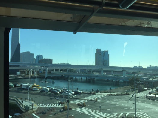
View from the monorail to the destination.
Finally, we reached the monorail station and headed to our destination – Miraikan. Miraikan also known as the National Museum of Emerging Science and Innovation, is Japan’s major science center located Daiba. Before, arriving our destination, we were able to take a photo with the huge unicorn Gundam in front of DiverCity Tokyo Plaza. The new life-sized Gundam statue is 19.7 metres! That is about xx times of my height! It was magnificent and exquisite. From this, I could sense the major interest of Japanese. After two days of experiencing the Japanese culture, I realised they were very psyched about figurines, cartoons and fantasies. This is very different from other countries where things that could psyche the whole nation was limited or hardly achieved.
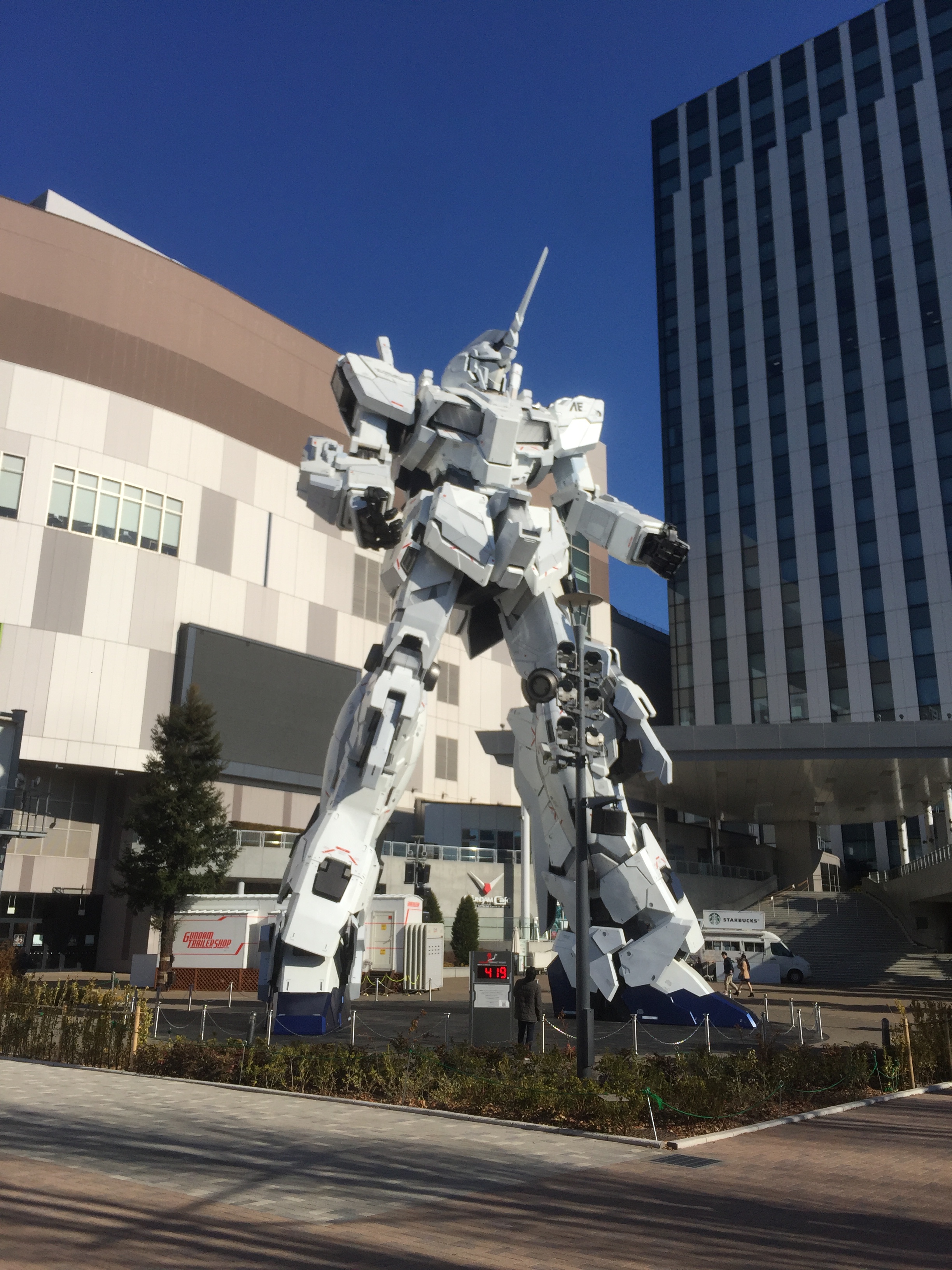
HUge gigantic statue!
Moving with our schedule, we got our tickets and proceeded to the science center. The group of us decided to start from the highest floor (5th) before proceeding to the 3rd floor. It was a wise and great decision as I enjoyed the exhibition better on the 5th floor than the 3rd floor. I am very interested in the universe, discovering the beginning of the universe, was it really the ‘Big Bang Theory’?
Through this exhibition, I was able to look into the universe, life and lab work. The study of universe was carried out by introducing observations on neutrino, the study on elementary particles and universe with the particle accelerator. There was a spaceship model, where they showcased the interior of a space shuttle. It was my first time being up close with the real space shuttle. There was a compartment for waste management, a dedicated personal room where their astronaut suit and personal entertainment can be found. Other than the spaceship model I only learn that Japan has come out with evacuation plans in case of a disaster. This is very applicable to Japan as Japan experiences huge temperature differences and more prone to diameters. Earthquakes, volcanic eruptions and other natural disasters have caused great damage to many lives. Plus, science, technology and transportation have developed bringing with them unexpected new types of disasters, as nuclear disasters, weather abnormalities and the spread of epidemic diseases. I felt that Japan make use of opportunities whenever possible and it was a learning experience each time a disaster happens.

Disaster repsonse step/learning outcomes.
After soaking up the knowledge on the 5th floor, we proceeded to the 3rd floor where we discovered our Earth. Using latest scientific data and tools, we were able to discover the connection between the planet and life. Is it then possible to make Earth sustainable
Overall the science center was very informative and is it possible to get educated despite the short exposure time at the science center.

Spectrophotometer components.
After lunch, we proceeded with Uneo where we explored the Museum of Natural Science. It was great to see how Japanese use science to interact with the museum visitors. Japan adopts a more interactive experiment based approach where visitors get to experience carrying out the experiments by themselves. Giving visitors the full control of the science, I had a deeper impression and memory of the area. Despite the short time duration allocated, I was able to connect with my limited Chemistry knowledge with Japanese words. There were a lot of inference made but to verify them, we had to google the setup and some concepts involved.
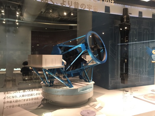
Telescope used for space observatory.
Overall today has been a fun, enriching but rush day. I hope I will be able to fully immerse and enjoy the Japanese culture in the days to come.

You must be logged in to post a comment.