
Ferris wheel near Odaiba

Akihabara

Miss that hot milk tea!

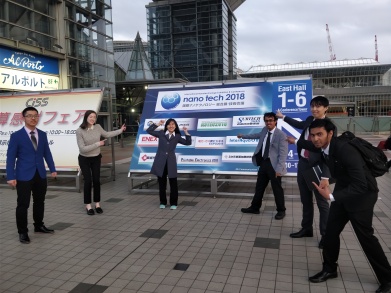
Nanotechnology Study Tour – 2018
La Trobe and NUS students visiting Tokyo, Japan in February 2018


The last blog is always the hardest. This is my third iteration of what started as 1000 word blogs explaining my thinking and reasoning behind participating in this tour, what I learnt from it and what’s next?. Hope you like it 🙂
The study was an epic roller coaster ride of experiences. Here’s some cool snaps you might have forgotten just to get you in the mood.


A collection of photos that capture Japan in its true elegance
My expectations of the study tour before it took place were pretty high to be honest. I expected to have loads of fun and make heaps of mates and learn about nanotechnology from and industrial and academic perspective. Truth be told I never thought it was going to be as WILD and WONDERFUL as it was. Visiting different parts of Tokyo and trying different Japanese food became a ritual from the first day for us and it was a great way to have fun and release the stress as well.
The study for me was a way of testing whether this field was still a hype from research findings and whether it was market ready. From all the booths I’ve come to the conclusion that nanotech still requires a lot more research before it’s market ready as a solution for the existing market needs (I know it’s a blunt and broad statement. What did you expect?). There’s so much more potential in the surrounding services and tools market such as printers ( 3-d or using CLIP technology) and microscopes.

LG showing off their CNT’s and Li ion battery
15/02/18
What’s next? Well I have no freaking clue!, but I know it’s going to be better than this. What I can tell you is what I will be focussing on for this year. This year I will be focussing on the supporting industries to nanotechnology such as the printing industry (3-d) / Sensors ( in general), microscopes and AI.
Life Tip: Approach anything with a vague idea of what can happen: that way you always leave space for things that you never imagine could happen: which is a LOT :).
Japan domo arigato for all the crazy and chaotic experiences you gave us. You will always be remembered.
 Off to Melb: Sayonara Japan
Nipun Amarasinghe,
Signing off,
Peace.

Alive on the other side
(somewhere in Ginza)
18/02/18
The day started off as usual with the routine meet up before we headed off to the nanotech exhibition. Today was film day; we had to film the intro, a couple of interviews and the ending.
We started by taking shots of the big sight and doing the introduction outside which was fairly arduous as it was cold and windy. The next in our list was a shot from the inside of Tokyo Big Sight, in front of the nanotech conference.
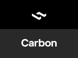
Next we started filming some other shots around the exhibition before heading off to do an interview with carbon. The interview with Carbon was off to a bad start as I forgot my mic and had to get it, however it turned out to be one of the best interviews conducted. It’s safe to say Carbon was my favourite company in the whole exhibition. For all those noobs Carbon is a printing company that uses a novel technology called CLIP (Continuous Liquid Interface Printing) which enables DLS (Digital Light Synthesis) to manufacture cool 3-d products.

Printing in action

An image explaining CLIP technology
Steven Kern the director, Japan support who we interviewed was a pretty chilled guy. He took the time to give us detailed explanations about the process and passion behind the product.
Afterwards we headed over to the German stall to interview them about Germany and the nanotech industry there. Then we roamed over to the next exhibition to get a quick idea about the production exhibition. It was filled with corporate giants such as Fujitsu and Noritake’.
As the saying goes ‘all good things must come to an end’ the Nanotech 2018 Study Tour officially ended today. I am excited at what lies ahead yet nostalgic of all the things experiences we’ve had and all the buddies we’ve met along the way :). I’d like to thank Dr.Paul, Goki, all my buddies and Team Pico for making this study tour successful and enjoyable.
Shout out to Team Pico for achieving an astounding feat: the best team eva!
 ]
]
G _ O TEAM PICO !
16/02/18
Check out this sick video on Carbon printing
Sayonara mates,
Nipun Amarasinghe.
 Keyence: the microscope company
15/02/18
Today was about making the most of time in the exhibition. We visited the Tokyo University (Komaba Campus). We had an information session at the university which was followed by lab visits. We were introduced the work of the two professors’. This includedKelvin Probe Force Microscopy (KFM), photo-thermal spectroscopy with Atomic Force Microscope (AFM), Magnetic Force Microscope (MFM), colour-AFM, and Field Ion Microscope (FIM). These tools form an important part of 2-D material analysis.

Colour Atomic Force Microscope (AFM)
15/02/18
Scanning Probe Microscope (SPM)
15/02/18
After the lab visits we headed to the nanotech expo. After roaming around for so long, I felt like I know all or most exhibitors by memory. We managed to secure an interview with LG on carbon nanotubes. Another two interviews were confirmed for tomorrow (one with Carbon – 3d printing, ITALIA -Italy booth). We were juggling between attending seminars and holding interviews.
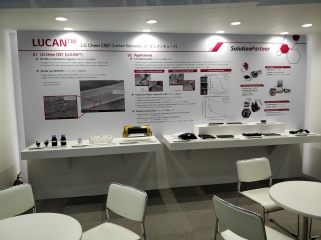
The LG stall promoting carbon nanotubes
16/02/18
A simple rant:
The product you sell can’t just be a little better than your competitors it has to be MUCH MUCH BETTER for consumers to choose your product over the existing competitors. A good company is a group of talented and passionate people with a single motive of helping people by providing a service or selling a product.
Underdogs like Carbon have a killer product and they add value to the market as their products are 20-100 times faster, isotropic and more durable than their competition. Their technology is called Continuous Liquid Interface Productions(CLIP). It is a method which uses light and oxygen to produce objects from a pool of resin.
Carbon – 3D printing
16/02/18
An important life tip I learned today was that when working in a group towards a common goal there will be disputes, it takes skill to be able to know when to compromise and when to completely reject an idea. There’s a cadence to it.
Hope you had an amazing time so far 🙂
Keep rocking it,
Nipun Amarasinghe.
–

The day started with us heading to University of Tokyo. The first on our agenda was an information about the degree programs and internship programs at University of Tokyo. It was conducted by a very friendly professor and it was very informative.
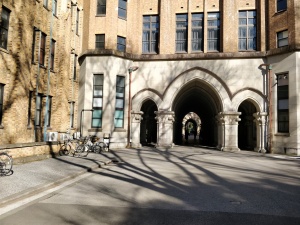
University of Tokyo
14/02/18
STM
14/02/18
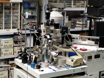
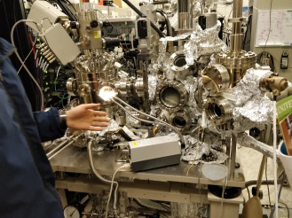
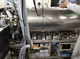
We visited two labs after the information session. The first lab we visited was interested in creating 1 atomic layer superconductors using scanning tunneling microscopes (STM). STM can be used for to measure and observe the sample without exposing it to air.
MH- RHEED (reflection high energy electronics detector present in the STM can be used to check the sample state). The STM has 4 point probes to measure conductivity. Research on two dimensional system mimicking superconductivity is important in the as it could be used in miniature electronics.
The next lab we visited was a quantum chemistry lab. This lab measured and tried to control ultra fast reactions typically in femto or pico second ranges. Electron diffraction method is used to measure the intermolecular distances. The system collides gas samples, gas beam and laser beam causing more energy shifts which can be used to measure the structure.
Machine used in the quantum chemistry lab
14/02/18
After the lab visits we visited the Nanotech 2018 expo held in the big sight. Here is an some interesting snap of our journey.
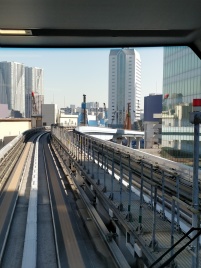
On our way to Tokyo Big sight
14/02/18
The Nanotech 2018 was an amazing experience. It had large companies such as LG, Shimadzu and NEC. The small companies such as Carbon were also present. The company I was most interested in was a small company called Carbon. The company uses programmable liquid resins, digital light and oxygen permeable optics to print materials. Carbons manufacturing process is really fast up to 100X faster than other additive manufacturing process. The adidas midsole is printed in 10 minutes, now that’s fast!. Carbon has the capability to print high – resolution with an excellent surface finish and isotropic mechanical properties. I really think there is potential for this company. Go have a look at Carbon.
 The Tokyo Big Sight
15/02/18
Till next time,
Nipun Amarasinghe.
 HAXPES
13/02/18
I’m gonna get straight to the point, this blog doesn’t have a real storyline attached to it like my other blogs do. So you’re more than welcome to tune out today and tune in tomorrow for the regular blog post.
The day started off with the group travelling to Tsukuba. The journey to Tsukuba was very uneventful with everyone having power naps to save energy for the rest of the day.
13/02/18
Information overload
The first half of the day was an information session about how cool it is to work for NIMS/MANA ( and how hard it it to get in to it too :p). We sat in an auditorium with cool foldable seats and were given a big bag of brochures, in case you don’t remember anything from the information session today morning which I’m gonna be honest I don’t and I’m pretty sure you don’t too.. :).
There was a lunch break after the session and the food in the cafeteria was phenomenal. The curry chicken was a real bang for the buck. NIMS is a definite must go for anyone coming to Tsukuba at least for the food :).
The latter half of the day comprised of us going to visit various labs inside MANA. The experiments conducted in the labs were really world class. I won’t mention all the labs since I’m pretty sure you can find further information from your friend Google. I loved the demonstration of the Scanning Probe Microscope.

Scanning Probe Microscope Model
14/02/18
With that I will end the blog.
Catch you tomorrow,
Nipun Amarasinghe

You must be logged in to post a comment.